dev-kit-2020
Dev-kit interfaces
The Chromation dev-kit divides into three interfaces:
- USB out
- SPI out
- Analog out
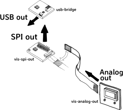
USB out
Chromation recommends using the USB interface for initial evaluation and instrumentation.
The dev-kit ships ready for USB connection to a computer.
Windows users enable Load VCP
Windows users connecting the dev-kit for the first time:
- open Device Manager
- locate
USB Serial Converter, right-click and selectProperties - on the
Advancedtab, check the box toLoad VCP
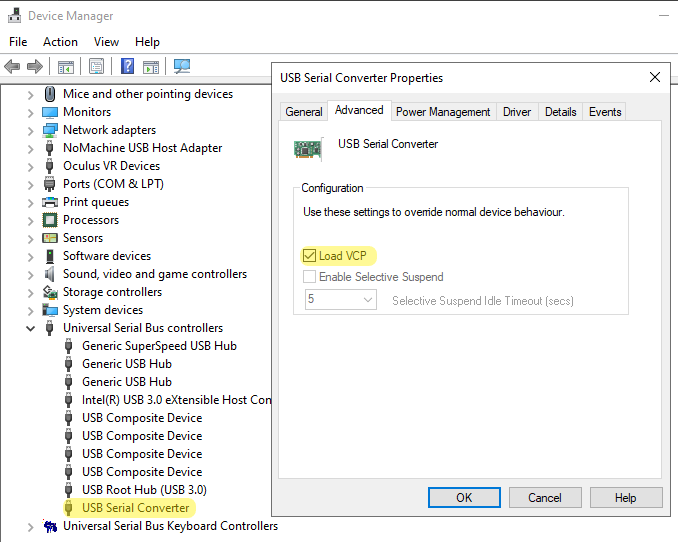
If Load VCP is not checked:
- the LabVIEW executable still runs
- but the Python API raises the following exception when it attempts to open communication with the dev-kit:
MicroSpecConnectionException: Cannot find CHROMATION device
Python and LabVIEW interfaces
Users communicate with the dev-kit using either:
- Python project
microspecon PyPI – Windows, Mac, Linux- see project here: https://pypi.org/project/microspec
- start using
microspecnow: jump to PYTHON.md
- LabVIEW GUI executable
dev-kit-2020-LabVIEW.exe– Windows only
Chromation recommends using Python to communicate with the
dev-kit. Chromation provides example scripts for using the API, a
command line interface for taking measurements, and a GUI
interface for taking measurements. In addition to the API,
project microspec includes tools to help developers interested
in modifying the API to run unit tests, emulate hardware, and
rebuild the documentation. All of Chromation’s Python code is
available for free under the standard MIT license.
Chromation provides the LabVIEW GUI but plans to discontinue using LabVIEW when a stable Python version of the GUI is released.
Analog dark correction
The dark signal has two components:
- DC offset
- this is called dark-offset or voltage-offset and is specified in Volts
- the offset varies on a per-pixel basis
- AC noise
- this is called dark-noise and is specified as mV RMS
- dark-noise limits precision in measuring the dark-offset
Chromation uses the term analog dark-correction to mean subtracting a single DC offset from the VIDEO signal to use the full dynamic range of the ADC. In other words, zero photons roughly shows up as a gray value of zero counts. See ENOB for details on ADC resolution and dynamic range.
The dev-kit is shipped with dark-correction turned on and dark-offset trimmed for an average dark of approximately 1.5% of full-scale (1000 counts out of 65535 counts) at 1ms exposure time. This setting is usually sufficient to eliminate the need for subsequent finer dark-correction in software.
For more accurate dark-correction, rotate the trimpot counterclockwise to subtract less of the dark offset. This reduces the amount of coarse dark-correction. Increase the offset (reduce the coarse dark-correction) until the dark measurement for all pixels is greater than zero counts in any single frame of data.
Fine-tuning the trim pot to get very close to zero counts is pointless. Using the Chromation dev-kit, there is plenty of extra dynamic range in the ADC, so it is even fine to turn off the analog dark-correction completely and do the coarse dark-correction in software. The advantage of hardware dark-correction is to reduce the number of measurements and simplify the software that analyzes the measurements.
To perform a fine dark-correction in software: collect an average dark measurement for subtracting from illuminated measurements. See details in Coarse and Fine dark-correction
Dark correction hardware in the dev-kit
The pixel voltage from the spectrometer chip, output on pin
VIDEO, is dark-offset-corrected using a reference voltage from
the spectrometer chip, output on pin VREF:
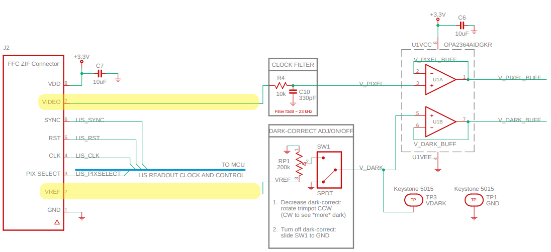
VIDEO changes with each pixel that is clocked out, but VREF
outputs a constant voltage (not a per-pixel voltage).
VREF is an over-estimate of the dark-offset. The trimpot forms
a simple voltage divider that takes a fraction of VREF for
doing an analog dark-correction.
The slider switch turns this analog dark-correction on/off. This is useful when comparing live data against data recorded without any dark-correction, or when performing all dark-correction in software.
SPI out and firmware programming
The dev-kit has two stacked PCBs:
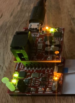
- the bottom PCB is
vis-spi-outvis-spi-outconverts the spectrometer chip into a SPI Slave
- the top PCB is
usb-bridgeusb-bridgeconverts the SPI interface to a USB interface
The names usb-bridge and vis-spi-out are used in the PCB
design files and in the firmware respository.
The connection between the usb-bridge and the vis-spi-out is
the 16-pin header:
There are a total of eight signals on this 16-pin header. Five
signals are the SPI interface. The other three signals are Power
(3.3V and 0V) and Reset. These signals also serve as the Flash
memory programming connections from the 6-pin shrouded header on
usb-bridge.
Five-wire SPI
This 16-pin header carries the five-wire SPI interface. Typicaly SPI interfaces only have four signals:
- Master-In Slave-Out (MISO)
- Master-Out Slave-In (MOSI)
- Slave Clock (SCK)
- Slave Select (SS)
The fifth SPI signal is Data Ready (DR). This is a Slave output to indicate to the Master when data is ready. For example, after the SPI Master commands the SPI Slave to capture a frame (a spectrum measurement), the SPI Master waits for Data Ready before reading the frame from the SPI Slave.
All pins duplicated for probing
Each signal is duplicated: eight signals, 16 pins. The pins are duplicated for two reasons:
- access to components on
vis-spi-out - probing the SPI bus
Reason 1: Access vis-spi-out
Orientation of usb-bridge on vis-spi-out does not matter! As
long as the pins line up, it is impossible to connect these two
PCBs the wrong way.
The dev-kit ships with the usb-bridge PCB directly above the
vis-spi-out PCB:
With power off, pull off the usb-bridge PCB and reconnect it
rotated (making sure that all 16 pins line up again):
- this gives access to parts on
vis-spi-outfor analog dark-correction:- the dark-correct trim-pot and on/off slide switch
- the dark-correct test point
- this also gives access to the two-pin female socket header:
- modify the firmware to use these two pins as either general purpose I/O or I2C communication
- coming soon: Chromation uses these two pins as general
purpse I/O for control of two LED boards we are adding to
the dev-kit: a high-CRI white and a broadband NIR
- jumper wires connect this header to the external-control header on the LED boards
- control the LEDs over USB via the Python interface (or
over SPI if you are connecting directly to the
vis-spi-outboard)
Reason 2: Probe the SPI bus on a scope or logic analyzer
- with power off:
- separate the two boards
- use jumper wires to connect the eight signals between the two boards
- probe signals on the duplicate pins
This example shows five jumper wires for SPI and two jumper wires
for power, connecting the vis-spi-out and usb-bridge. The
RST signal is not jumpered because it is only needed during
firmware programming.
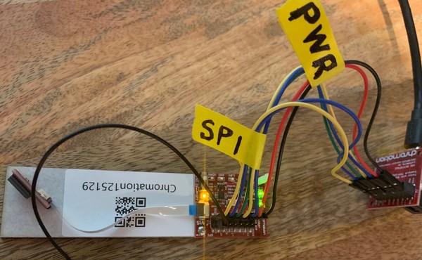
The bottom row of spare pins on vis-spi-out are the duplicate
pins for probing.
One black jumper wire is shown on the bottom row, leftmost. This
is the duplicate of the GND signal on the top row, rightmost.
The jumper wires are female-to-male, for example Adafruit #1954
. The female end is
for inserting on the vis-spi-out header pins.
16-pin header includes the 6 Atmel ISP connections
Six of the eight signals also double as microcontroller Flash memory programming signals for Atmel’s In-System-Programming (ISP):
- 3.3V
- 0V
- Reset
- MISO
- MOSI
- SCK
The usb-bridge board has a shrouded ISP header that mates with
the standard Atmel 6-pin, ribbon cable, programming connector.
Use any Atmel AVR programmer. Chromation uses the Atmel-ICE, but an AVRISP-mkII or any AVRISP-mkII imitator works just as well.
You can program either board (usb-bridge or vis-spi-out) from
this shrouded 6-pin header on the ubs-bridge board. You do not
need to separate the boards to program the vis-spi-out board.
The slide switches on the usb-bridge select normal-mode (SPI)
or programming mode (ISP), and select which board is being
programmed. Details on the slide-switch settings and make
commands are in the firmware programming doc.
Spi Slave configuration and protocol
The SPI Slave configuration (clock polarity and phase) and
command protocol are documented in the firmware repository in
the SpiMaster.h
header.
Specifically, see the documentation for function
SpiMasterInit().
The SPI Slave follows the protocol defined in microspec.json in
Chromation’s microspec project on PyPI. The JSON file is also
available from the microspec repository on
GitHub.
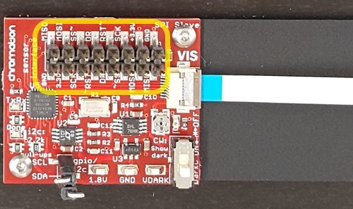
Analog out
Analog out is the direct output from the spectrometer chip.
Spectrometer chip
In production, the user assembles the spectrometer chip directly on their PCB.
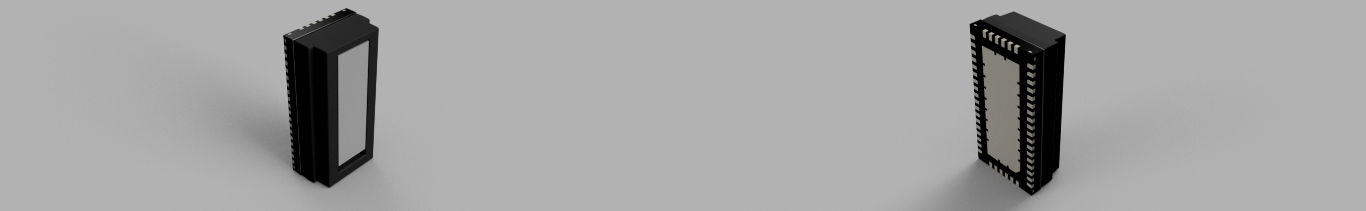
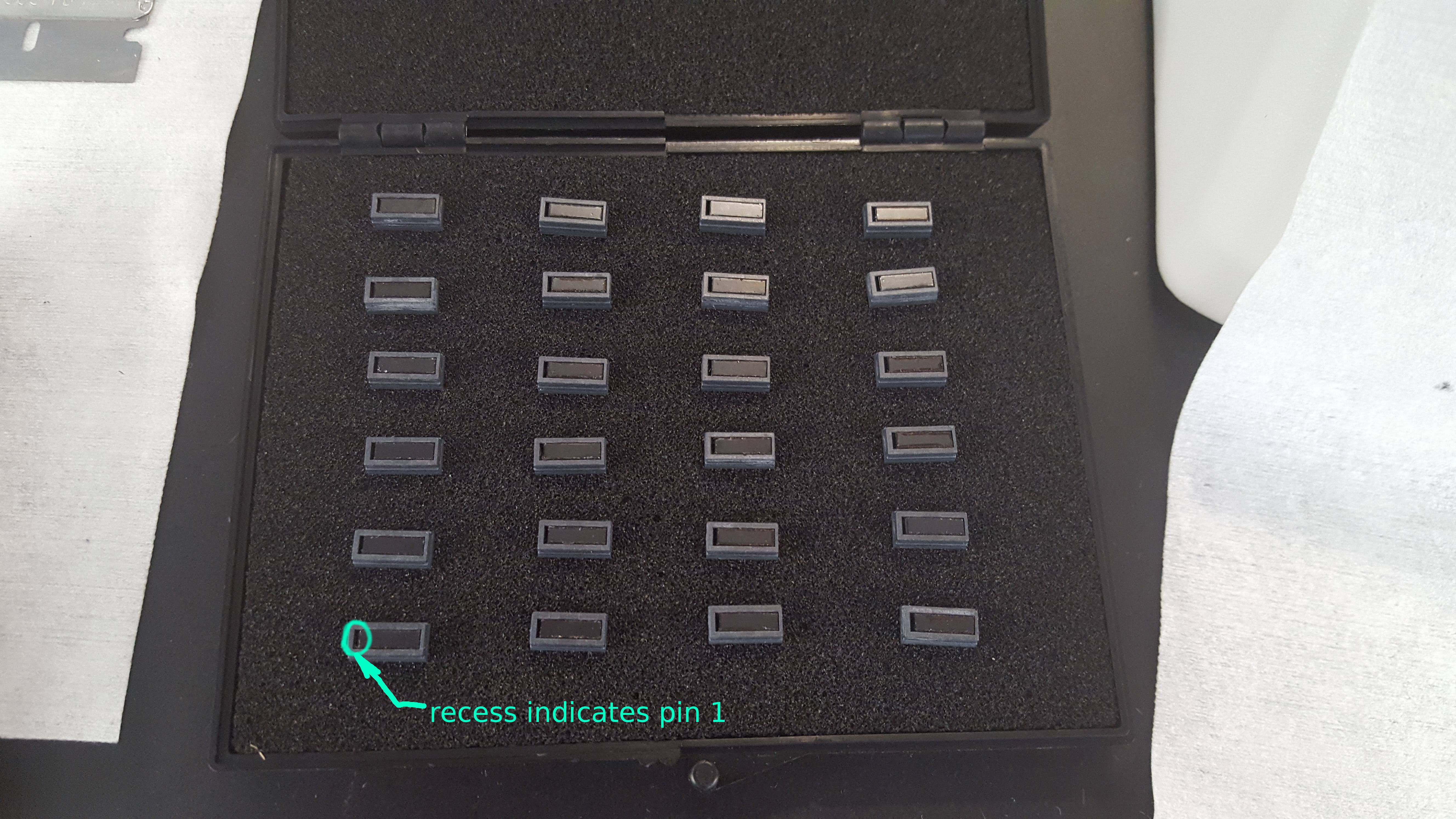
The package is a 48-pin QFN, but only nine pins are used, two of which are the 0V reference (ground), so there are only eight signals in total.
The top of the package is an optical die coated in a black absorber. There is a visible gap or recess at one end of the optical die. This is where light enters for spectrum measurements.
This recess/gap feature is also used during PCB assembly to identify this side of the QFN as the pin 1 side.
Access chip pins in dev-kit with ZIF connector
The dev-kit spectrometer is mounted on breakout board
vis-analog-out for connecting via a zero-insertion-force (ZIF)
connector:

To design a PCB that connects to vis-analog-out, use the same
ZIF connector, Hirose
FH12-8S,
or any similar flat-flexible-cable (FFC) connector with 0.5mm
pitch.

FFC Cables
FFC Molex# 15166-0078 connects the two ZIF connectors.
FFC specifications:
- 8-conductors
- 0.5mm-pitch
FFC cables come with the contacts on the same side or opposite
sides. The FFC in the dev-kit has opposite-side contacts so that
the vis-spi-out PCB has its ZIF connector on the PCB top,
while the vis-analog-out (breakout) PCB has its ZIF connector
on the PCB bottom. This way the spectrometer chip sits
right-side-up without twisting the FFC.
Spectrometer Interface PCB
For users that design their own PCB to interface directly with
the spectrometer chip, here is a summary of what vis-spi-out
does:
- analog-to-digital (ADC) conversion of the pixel voltages
- digital I/O:
- configure the chip’s internal analog connections
- control pixel exposure time
- coordinate pixel readout with the ADC
See the vis-spi-out schematic for details.
Also see the vis-spi-out firmware source code, in particular:
firmware/lib/src/Lis.hfirmware/lib/src/LisConfig.hfirmware/lib/src/LisConfigs.h
The name Lis refers to the linear photodiode array in the
spectrometer chip.
Appendix
ENOB
Effective Number of Bits (ENOB) is the effective number of bits of ADC resolution for the complete system. The ADC is one part of this system. The dev-kit uses a 16-bit ADC, but the effective number of bits is not 16. The limiting factor for ENOB in spectrometers using CMOS image sensor spectrometers, such as the Chromation spectrometer, is the image sensor itself.
In qualitative terms, this means that image sensor read noise well-exceeds the voltage step per ADC bit using a 16-bit ADC.
For reasonable measurement bandwidth, spectrometers using CMOS
image sensors take advantage of 13 effective bits of resolution
at most. The ENOB for the image sensor in Chromation#
CUVV-45-1-1-1-SMT is 11 bits.
The limitation is the SNR of the CMOS image sensor. SNR is the ratio of Vsat to read noise. Vsat is the maximum output swing minus the offset voltage (offset voltage is sometimes called the dark offset). Read noise is the AC noise component in the illuminated signal.
For the CMOS image sensor in CUVV-45-1-1-1-SMT:
- Vsat = 1.95V
- the pixel charge to voltage conversion factor is 6.5µV/electron
- voltage at full-well is 3.0e5 electrons x 6.5µV/electron = 1.95V
- with a 3.0V maximum swing, expect about 1.05V of offset voltage
- read noise = 1.5mV RMS
SNR = 1300 (1.95 Vsat / 0.0015 mV RMS)
Following the convention in section 6.6 of EMVA1288, express SNR
in dB using 20*log10(SNR):
SNR = 62.3 dB
The dev-kit uses a 1.8V ADC reference, reducing the SNR. There are two good reasons for doing this:
- for design simplicity, 1.8V is a standard reference voltage value
- Vsat does not take into account the linear operating range of
the pixel
- linear operating range is not 100% of the full-well capacity
- therefore, sacrificing SNR improves spectrometer linearity
Linear range as a percentage of the pixel’s full-well capacity is
usually not documented, but for the image sensor in
CUVV-45-1-1-1-SMT sensitivity is linear between 5% and 70% of
full-well. The 1.95V value corresponds to 100% full-well. Using a
1.8V ADC reference clamps the maximum gray value (65535 counts)
at 92% of full-well (and then the maximum guaranteed linear
gray value is around 50000 counts).
Using 1.8V as the actual Vsat, the ENOB of the image sensor for this reduced voltage range is:
SNR = 1200 (1.8 Vsat / 0.0015 mV RMS)
SNR = 61.6 dB
ENOB is calculated as log2(SNR):
ENOB = log2(1200) = 10.2 bits
Rounding up to the next whole number, this is 11 bits.
To take full advantage of this SNR, therefore, the analog front-end (ADC, ADC voltage reference, and op-amp buffers) needs an ENOB in excess of 11 bits.
Coarse and Fine dark-correction
Applications do not always need a fine dark-correction step. This section explains the cost-benefit on implementing fine dark-correction. Please contact Chromation if you would like more detail.
Some image sensor manufacturers call the DC offset a dark-offset, others call it a voltage-offset. These are identical – it is just the DC offset in the VIDEO signal.
The dark offset only affects dynamic range and SNR to the extent that it limits the maximum swing of the VIDEO signal. This offset does not set the noise-floor. It is a DC value and has nothing to do with noise.
Noise is time varying. As a single value, it is specified as mV RMS. Given the usual AWGN assumption about the distribution of the noise, this RMS value is the standard deviation when looking over many frames of data; when watching raw live data with very short exposure time, the peak-to-peak noise riding on the signal is about 6x this RMS value (because 99.7% of the readings are within three standard deviations of the mean value).
For the Chromation dev-kit, 6x the RMS read-noise is about 328 counts.
The magnitude of the dark noise and the illuminated noise are different. Manufacturers refer to noise in the illuminated signal as read noise. Use dark noise to determine the image sensor’s dynamic range. Use read noise to determine the image sensor’s SNR.
- dark-offset is reduced by subtracting:
- the dev-kit ships with a single voltage offset subtracted from all pixels
- for finer dark-correction, determine the remaining average dark offset on a per-pixel basis and subtract this offset in software
- dark-noise is reduced by filtering
- filter the dark-noise to find the per-pixel dark offsets to
subtract:
- to determine the per-pixel values to use in fine dark-correction, the dark-signal must be low-pass filtered to get a value closer to the “true” DC-offset
- at long exposure times, the signal is already effectively low-pass filtered, at short exposure times it is necessary to average frames
For general use cases, such as the qualitative measurements done in the initial stages of application development, Chromation’s “analog dark-correction” is sufficient. This is a “coarse” dark-correction. It subtracts the same value from all measurements.
The dev-kit ships with the dark-correct trim-pot set to a good default setting for this general use case.
A finer dark-correction step is sometimes necessary when the data is being scaled (i.e., multiplying the pixel gray values by a constant or a wavelength-dependent array of values). This need arises at a further stage of application development where the measurement setup is known and the goal is to reduce the measurement error.
The source of error is that the dark signal does not scale with the illuminated signal. For example, doubling integration time (roughly) doubles the illuminated signal, but has very little effect on the dark signal. Therefore, on a pixel-by-pixel basis, any offset (positive or negative) introduces an additive offset that throws off calculations where the pixel value is scaled.
Typical examples where applications scale data are:
- normalizing by exposure time
- scaling all pixels by the integration time to compare two measurements taken at different integration times
- weighting the pixels with spectral irradiance calibration
coefficients
- each pixel is weighted by its own coefficient to convert gray values to spectral irradiance
Dark-correcting too much or too little introduces the same magnitude of offset error. Since the “coarse” dark-correction applies the same offset to all pixels, the best the coarse dark-correction can achieve is to have some pixels over-compensated and some under-compensated.
When adding a “fine” dark-correction step, let the “coarse” dark-correction under-correct all pixels (the dark-data never falls below zero counts on any pixel). The “fine” dark-correction then subtracts different offsets on a per-pixel basis to get all pixels as close as possible to having zero-offset.
Perfect dark-correction is impossible. There is always some offset error. The goal is just to make this contribution insignificant compared with other sources of measurement error.
The cost of fine dark correction is that measurements require an additional dark-correction step: determine the measurement integration time, collect many frames of dark data, average these frames, subtract this average from the illuminated measurement.
The number of frames to average depends on the exposure time: short exposure times require many frames, long exposure times may not require averaging at all. Ignoring the dependency of the dark signal on integration time, averaging frames and exposing for longer integration times have the same effect on the measurement bandwidth.
So do not start with a magic number like 100 frames to average. Instead, pick a target measurement bandwidth. For example, say the target measurement bandwidth is 1 measurement per second and the application has a bright target measured at 10ms and a much darker target measured at 100ms. Average 100 frames of dark to dark-correct the 10ms target and 10 frames of dark to dark-correct the 100ms target. The measurement bandwidth in both cases is 1Hz, so both dark measurements filter the same amount of dark noise.
“Fine” dark-correction only reduces the additive offset caused by the dark signal. If this error is swamped by other variables, “fine” dark-correction may not be worth the effort.
The added benefit of the “fine” dark-correction is that it acts on a pixel-by-pixel basis, as opposed to the “coarse” dark-correction which subtracts the same offset from all pixels (regardless of whether coarse dark-correction is done in hardware or software). Keep in mind that even when scaling data is required, this “fine” step may not be necessary or worth the extra effort.
If the extra accuracy of “fine” dark-correction is required, but collecting dark data is not practical, one solution is to collect the dark data ahead of time at many integration times, and then use a look-up table to select the correct dark-correction data.