dev-kit-2020
Design notes for vis-spi-out

This is not an explanation of the design, just documentation on some design decisions.
Power
- power all parts on single +3.3V supply
- +3.3V from voltage regulator on
usb-bridge
ADC
ADC Voltage reference
- ADC voltage reference is 1.8V
- TI# LM4132AMF-1.8/NOPB
- 1.8V is a compromise between linearity and dynamic range
Linearity
- detector manufacturer guarantees linear response from 5% to 70% of full-well
- voltage at full-well capacity:
- 3e5 electrons x 6.5µV/electron = 1.95V
- this is 100% full-well
- 70% full-well is 1.365V
- (1.365/1.8) x (2^16-1) = 49697 counts
- 1.8V is 92% full-well
- from 49697 counts to 65535 counts (1.365V to 1.8V), the response is not guaranteed to be linear
- if not linear, the response is soft-saturated
- Chromation has not characterized this behavior, but qualitatively we have not observed any distortion
Dynamic range
- the tradeoff is that lowering the ADC voltage reference also decreases dynamic range, defined as the ratio of the largest output voltage to the output voltage where SNR=1
No hard-clipping below full-scale
- the response is guaranteed not to hard-clip below full-scale
(65535 counts)
- the full-swing voltage of VIDEO is 3.0V:
- the 3.3V rail minus 0.3V
- this swing includes the offset voltage
- maximum offset voltage is 1.1V, typical is 0.84V
- adding the maximum offset voltage to the 1.8V ADC voltage reference, the total is 2.9V
- 2.9V is 100mV below the 3.0V where hard-clipping occurs
- therefore, a full-scale 1.8V output should never hard-clip below full-scale
- the full-swing voltage of VIDEO is 3.0V:
Package
- Device
LM4132AMF-1.8/NOPB- Package Type
SOT-23 - Package Drawing
DBV - Pins
5
- Package Type
Circuit Connections
- tie
ENpin toVINpin - use two capacitors: CIN and COUT
- satisfy: CIN >= COUT and COUT < 10 µF
- make CIN 10 µF and COUT 1 µF
Dark-correction
Overview
The dark signal has two components: a DC offset called dark-offset and an AC component called dark-noise.
- dark-offset is reduced by subtracting:
- determine the average dark offset on a per-pixel basis
- subtract these per-pixel offsets from the illuminated measurement
- dark-noise is reduced by filtering:
- filtering decreases the measurement bandwidth
- filter by:
- averaging frames
- using longer exposure times
The goal of dark correction is to eliminate the dark signal prior to subsequent data processing for radiometric analysis (i.e., comparing spectral power across wavelengths and/or across measurements). Even in applications that are pure wavelength detection, eliminating the dark signal is desirable because it improves dynamic range.
The pixel voltage from the spectrometer chip, output on pin
VIDEO, is dark-offset-corrected using a reference voltage from
the spectrometer chip, output on pin VREF:
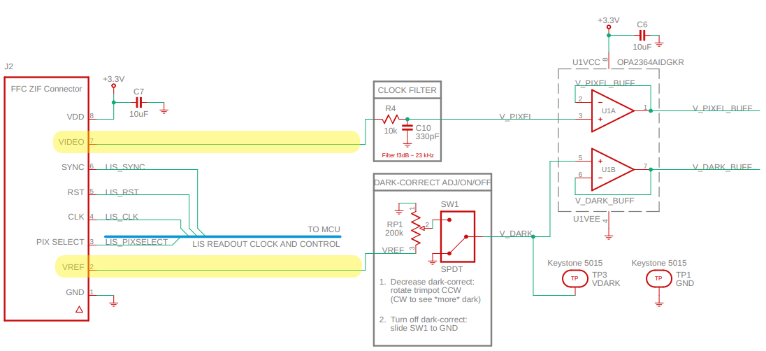
VIDEO changes with each pixel that is clocked out, but VREF
outputs a constant voltage (not a per-pixel voltage).
VREF is a slight over-estimate of the dark-offset. The trimpot
forms a simple voltage divider that takes a fraction of VREF
for doing an analog dark-correction. The slider switch turns this
analog dark-correction on/off.
The dev-kit is shipped with dark-correction turned on and dark-offset trimmed for an average dark of approximately 1.5% of full-scale (1000 counts out of 65535 counts) at 1ms exposure time. This setting is usually sufficient to eliminate the need for subsequent dark-correction.
For users that need more accurate dark-correction, rotate the trimpot counterclockwise to subtract less of the dark offset. This uses the analog dark-correct as a coarse dark-correction. Perform the final fine dark-correction in software the usual way: collect a dark measurement for subtracting from the illuminated measurement.
dark-correct trimpot design notes
- VREF analog output impedance is
10 kΩ - a 200 kΩ pot yields at most 95% of
VREF - layout: do not route traces under the pot
- would rely on the soldermask as an insulator
- the turn on the trimpot is metal, electrically connected to the wiper
- the underside of the trim is also metal, also connected (the turn mechanism is a single piece)
- it is OK to attach the pot directly to LIS-770i pin
VREF:- pot slightly loads
VREF:- the pot still has 95% of the
VREFvoltage across it
- the pot still has 95% of the
- pot slightly loads
- pot goes before the op-amp buffer
- op-amp inputs should have no problem avoiding loading even
the worst-case ouput impedance of this trimmed
VREFsignal - worst-case is with pot about midway
- then output impedance of trimmed
VREFis about 100 kΩ
- op-amp inputs should have no problem avoiding loading even
the worst-case ouput impedance of this trimmed
- even if
VREFoutput impedance with pot were somehow the full 200 kΩ of the pot, what is the op-amp input impedance?- op-amp is
TI# OPA2364 - input bias current is 10 pA
- 10 pA is insignificant:
- (V/kΩ) = mA
- mA * 1.0e6 = pA
- (V/kΩ)*1.0e6 = pA
- 0.5 / 200 * 1.0e6 = 2500.0 pA
- op-amp is
dark-correct on/off switch design notes
- slide switch for customers to turn dark-correction on/off without touching the trimpot
- switch connects
VDARKtoGNDinstead of pot wiper