dev-kit-2020
Design notes for vis-analog-out

CUVV-45-1-1-1-SMT pinout
Most of the pins on the QFN-48 are not used
The linear photodiode array IC in CUVV-45-1-1-1-SMT only has eight pads, but the CUVV-45-1-1-1-SMT package is a QFN-48.
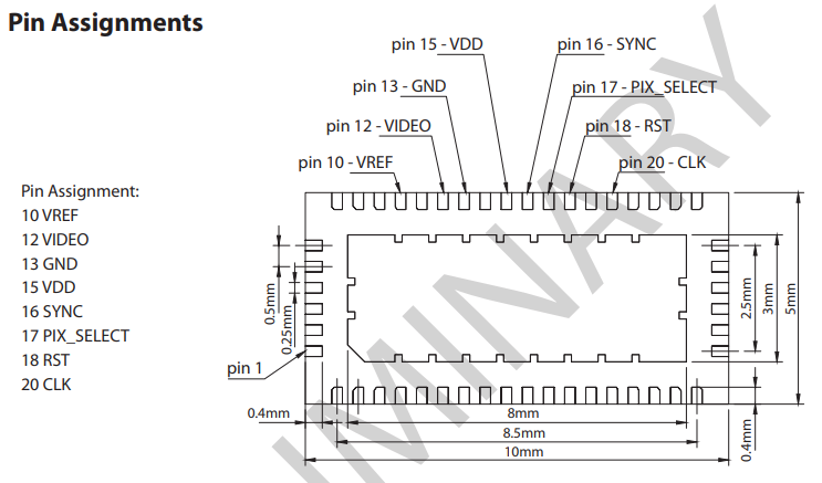
Nine of the 48 pads are used: the eight that connect to the
photodiode array, plus a ninth pad labeled SHLD (short for
“electrostatic shield”) that connects to the leadframe of the
QFN-48.
Tie SHLD to GND
SHLD is pin 14, right next to GND on pin 13. SHLD is not
shown in the above pin assignment drawing.
Connect the QFN-48 leadframe to the 0V reference (i.e., connect pins 13 and 14) and, if possible, tie the 0V reference to a copper plane on the PCB.
Intent of shielding
This creates a pair of conductor planes (the PCB copper plane and the QFN-48 leadframe) with both planes held at the same potential. This configuration helps reduce coupling of electrical noise into the charge amplifier circuitry of the photodiode array by preventing electrostatic coupling from below the spectrometer chip.
Breakout board mounting
The breakout board is designed to press-fit into a laser-cut slot. This is how Chromation ships the breakout board in the dev-kit.
Alternatively, the PCB has two holes for fastening to a housing.
FFC
Use FFC with opposite-side contacts
The ZIF connect on vis-analog-out is wired for connecting to
the ZIF on vis-spi-out using a flat-flex cable with
opposite-side contacts.
vis-spi-outZIF is mounted on the PCB top-side (the component side)vis-analog-outhas CUVV-45-1-1-1-SMT on the top-side and ZIF on the bottom side- an FFC with opposite-side contacts connects these two boards so that the CUVV-45-1-1-1-SMT sits face-up
FFC specs and general info
- FFC part number is Molex# 151660078 available from Mouser# 538-15166-0078
- 76mm long
- 8 circuits
- 0.5mm-pitch
- opposite-side contacts
- manufactured by Molex
- learn more about FFC on the Molex website